- 您现在的位置:买卖IC网 > Sheet目录1213 > EVAL-AD74111EBZ (Analog Devices Inc)BOARD EVAL FOR AD74111
�� ��
��
��EVAL-AD74111EB�
�EVALUATION� BOARD� SOFTWARE�
�DSP� EXAMPLES�
�The� following� text� gives� some� code� examples� showing� methods�
�of� interfacing� the� AD74111� to� Analog� Devices,� Inc.’s� fixed-point�
�DSPs.� The� flowcharts� are� generic� and� should� be� adaptable� to�
�any� type� of� DSP,� but� the� code� samples� are� specifically� for� the�
�ADSP-218x� DSPs.�
�INTERRUPTS�
�The� code� examples� that� follow� make� use� of� the� serial� port�
�(SPORT)� transmit� and� receive� interrupts� that� allow� the� processor�
�to� service� the� codec� only� when� required.� The� transmit� section�
�of� the� ADSP-218x� SPORT� consists� of� a� transmit� register,� Tx0�
�for� SPORT0� and� Tx1� for� SPORT1,� and� a� serial� shift� register,� Rx0�
�for� SPORT0� and� Rx1� for� SPORT1.� Transmission� of� a� data-word�
�is� initiated� by� loading� it� to� the� appropriate� Tx� register.� The� DSP�
�begins� transmitting� this� word� by� copying� it� to� the� serial� shift�
�register� where� it� is� clocked� out� one� bit� at� a� time� dependant� on�
�the� SCLK� rate.� A� transmit� interrupt� occurs� when� it� is� safe� to�
�load� the� Tx� register� with� the� next� value� to� be� transmitted.� The�
�DSP� will� not� allow� the� second� word� to� be� transmitted� until� the�
�first� word� is� completely� transmitted.� A� transmit� interrupt�
�occurs� when� the� second� bit� of� the� data-word� is� transmitted.�
�A� receive� interrupt� occurs� when� a� complete� data-word� is�
�received� into� the� Receive� Register� Rx0� or� the� Receive� Register�
�Rx1.� The� receive� section� of� the� SPORT� has� a� similar� serial� shift�
�register� to� the� transmit� section.� It� is� important� that� any� data�
�received� in� the� Rx� register� be� read� as� soon� as� possible� because� a�
�new� word� can� be� read� into� the� serial� shift� register� and� overwrite�
�the� Rx� register� once� the� entire� word� is� received.�
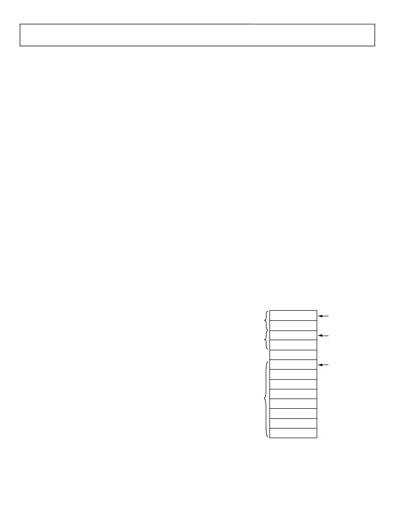
�The� software� uses� three� buffers� to� control� the� flow� of� information:�
�1.� The� control� buffer� contains� the� control� register� words� that�
�need� to� be� sent� to� the� AD74111.�
�2.� The� Tx� buffer� contains� a� control� register� value� and� a� value� for�
�the� DAC.�
�3.� The� Rx� buffer� stores� the� status� information� and� the� ADC� result.�
��When� the� program� is� running,� the� transmit� interrupt� reads� the�
�next� value� in� the� Tx� buffer� and� transmit� it� when� it� receives� a�
�transmit� interrupt.� The� receive� interrupt� does� most� of� the� work�
�in� this� example.� When� a� receive� interrupt� is� generated,� the�
�program� reads� the� value� from� the� Rx1� register� into� the� AY1�
�register� immediately� storing� it� for� later� use.� It� then� decrements�
�and� checks� a� counter� value� to� determine� how� many� receive�
�interrupts� have� been� received� in� the� current� sample� interval.� If�
�the� value� is� not� zero,� the� control� word� just� finishes� transmitting,�
�and� the� status� word� is� just� received.� The� status� information� is�
�not� required� in� this� example;� therefore,� the� program� returns� from�
�the� interrupt� subroutine� and� waits� for� the� next� interrupt� event.�
�When� the� program� determines� that� two� receive� interrupts� have�
�occurred� (control� counter� =� 0),� it� will� get� the� next� control� word�
�to� be� sent� to� the� codec� from� control� buffer� and� load� it� to� the�
�CTRL� memory� location� in� the� Tx� buffer.� The� ADC� value� that�
�was� just� received� is� copied� to� the� DAC� memory� location� to�
�create� a� loopback� operation,� and� this� value� is� transmitted� to�
�the� DAC� in� the� next� sample� interval.� The� program� resets� the�
�control� counter� variable� and� returns� from� the� interrupt�
�subroutine� to� wait� for� the� next� interrupt� event.�
�16-BIT� MIXED� MODE,� 16-BIT� DATA,� MASTER� MODE�
�The� flowchart� in� Figure� 6� is� an� example� of� how� to� interface� the�
�DSP� to� the� AD74111� in� master� mode.� In� master� mode,� the�
�codec� generates� the� DFS� and� DCLK� signals� so� the� TFS1/RFS1�
�and� SCLK1� are� inputs� to� the� DSP.� The� codec� is� operating� in� its�
�default� 16-bit� mixed� mode� with� the� data-word� length� set� to� 16�
�bits.� In� this� mode,� the� AD74111� generates� two� DFS� pulses� per�
�sample� interval,� one� for� the� control� register/status� information,�
�and� one� for� the� DAC/ADC� data.�
�Rx�
�Tx�
�STATUS�
�ADC�
�CTRL�
�DAC�
�CONTROL� COUNTER�
�REG� DATA� 1�
�REG� DATA� 2�
�I1�
�I2�
�I1�
�REG� DATA� 3�
�These� software� examples� take� the� ADC� results� and� send� them�
�back� to� the� DAC� to� create� a� loopback� effect.� The� DAC� output� is�
�therefore� one� sample� interval� behind� the� ADC� input.�
�CONTROL-�
�BUFFER�
�REG� DATA� 4�
�REG� DATA� 5�
�REG� DATA� 6�
�REG� DATA� 7�
�REG� DATA� 8�
�Figure� 5.� Buffer� Memory� Map�
�Rev.� 0� |� Page� 4� of� 16�
�发布紧急采购,3分钟左右您将得到回复。
相关PDF资料
EVAL-AD7741/42EBZ
BOARD EVAL FOR AD7741/7742
EVAL-AD8003-3CPEZ
BOARD EVALUATION AD8003-3CPEZ
EVAL-AD9830EBZ
BOARD EVALUATION AD9830
EVAL-AD9833SDZ
BOARD EVAL FOR AD9833
EVAL-AD9834SDZ
BOARD EVAL FOR AD9834
EVAL-ADAU1401AEBZ
BOARD EVAL FOR ADAU1401A
EVAL-ADCMP564BRQZ
BOARD EVALUATION ADCMP564BRQZ
EVAL-ADE7169EBZ-2
BOARD EVALUATION FOR ADE7169F16
相关代理商/技术参数
EVAL-AD74122EB-U1
制造商:Analog Devices 功能描述:- Bulk
EVAL-AD7414/15EB
制造商:AD 制造商全称:Analog Devices 功能描述:【0.5C Accurate, 10-Bit Digital Temperature Sensors in SOT-23
EVAL-AD7414/15EBZ
功能描述:BOARD EVALUATION FOR AD7414/15 RoHS:是 类别:编程器,开发系统 >> 评估板 - 传感器 系列:- 产品培训模块:Lead (SnPb) Finish for COTS
Obsolescence Mitigation Program 标准包装:1 系列:-
EVAL-AD7416/7/8EB
制造商:Analog Devices 功能描述:EVALUATION BOARD I.C. - Bulk
EVAL-AD7416/7/8EBZ
功能描述:BOARD EVALUATION FOR AD7416/7/8 RoHS:是 类别:编程器,开发系统 >> 评估板 - 传感器 系列:- 产品培训模块:Lead (SnPb) Finish for COTS
Obsolescence Mitigation Program 标准包装:1 系列:-
EVAL-AD7416EB
制造商:AD 制造商全称:Analog Devices 功能描述:10-Bit Digital Temperature Sensor (AD7416) and Single/Four-Channel ADC (AD7417/AD7418)
EVAL-AD7417EB
制造商:AD 制造商全称:Analog Devices 功能描述:10-Bit Digital Temperature Sensor (AD7416) and Single/Four-Channel ADC (AD7417/AD7418)
EVAL-AD7418EB
制造商:AD 制造商全称:Analog Devices 功能描述:10-Bit Digital Temperature Sensor (AD7416) and Single/Four-Channel ADC (AD7417/AD7418)